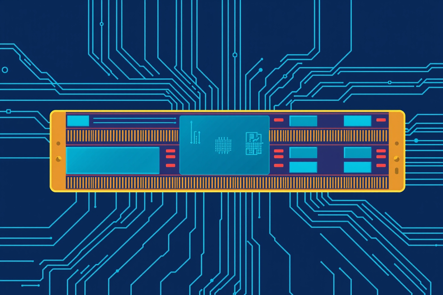
- What it is: Near-memory compute places processing elements adjacent to or inside the memory stack, so weight data is multiplied by activations before it traverses the off-chip bus, not after.
- Why it matters: autoregressive decode is bandwidth-bound at batch size 1. A 70B FP16 model loads roughly 140 GB of weights per second of inference, and the fastest HBM3E stacks available as of early 2026 cap at around 1.2 TB/s per device. The compute sits idle waiting for data.
- The gotcha: the memory wall is not a single wall. PIM DRAM solves weight-movement cost; it does not solve the KV-cache growth problem or the prefill compute bottleneck, both of which demand separate treatment.
Who this is for: hardware-aware ML engineers, inference infrastructure architects, and systems researchers who want to understand where near-memory compute fits in the transformer serving stack, what real devices exist today, and what the software gap actually costs. You should be comfortable with memory hierarchy concepts and have some familiarity with transformer inference mechanics (prefill vs. decode, KV-cache, attention). This is not a getting-started guide to transformers.
The weight-loading problem, stated concretely
Picture a production serving cluster running a 70B-parameter model in FP16. A new token generation request arrives. The decode step requires every one of the model’s weight matrices to stream through the memory bus and into the tensor cores exactly once: roughly 140 GB of data for a single generated token, regardless of whether the batch contains one request or a hundred. At batch size 1, that token takes whatever the memory bandwidth allows. At batch size 64, the same weight loads are amortized across 64 requests, so the cost per token falls by 64x.
Latency-sensitive interactive serving cannot wait for large batches to accumulate. An SLA of 50ms per token and a median inter-token gap of 40ms leaves almost no room for batching. You are, functionally, always operating at small effective batch sizes for latency-bound traffic. That means you are almost always memory-bandwidth-bound.
The standard A100 SXM provides 2 TB/s of HBM2e bandwidth and 312 TFLOPS of FP16 compute. The arithmetic intensity of a matrix-vector multiply at batch size 1 is roughly one FLOP per two bytes loaded, which means peak utilization under those conditions is around 2% of peak FLOPS. The hardware is delivering about 2 cents of compute value for every dollar of silicon you paid for. The H100 SXM with HBM3 does better on bandwidth (3.35 TB/s) but the ratio does not change fundamentally: more bandwidth is the right investment, not more FLOPS.
Near-memory compute attacks this ratio directly, by reducing the distance data must travel before a multiply-accumulate can happen.
How NMC architectures actually work
The memory wall shows up because moving data is energetically expensive and serialized. Every byte that crosses the off-chip bus between HBM and the host die travels through package-level interconnects, across a memory controller, into the host chip’s L2 or SRAM, and finally to a functional unit. At the bandwidths needed for large language models, that path is the system’s bottleneck.
NMC addresses this in three structurally different ways, shown in Figure 1.
graph TD
    subgraph "Processing-in-memory (PIM)"
        A[DRAM bank] --> B[In-bank MAC units]
        B --> C[Result bus to host]
    end
    subgraph "Near-memory (2.5D tile)"
        D[HBM stack] --> E[Compute tile in same package]
        E --> F[Reduced off-package traffic]
    end
    subgraph "Bandwidth-first ASIC"
        G[On-chip SRAM fabric] --> H[Dataflow tensor cores]
        H --> I[High-utilization execution]
    end
Figure 1. Three NMC architectural approaches and where compute lands relative to the memory stack. Look for how far the multiply-accumulate unit sits from the data: closer means fewer bytes cross the bottleneck bus.
Processing-in-memory (PIM) DRAM places compute inside the DRAM die itself, adjacent to the memory banks. Samsung’s HBM-PIM (released 2021, with subsequent iterations) and SK Hynix’s AiM (Accelerator-in-Memory) both follow this model. Each bank or bank group gets a small set of multiply-accumulate units. When a weight vector lives in those banks, the dot product with an activation vector can execute inside the chip, and only the result (a scalar) needs to cross the bus. For a 4096-element weight row in FP16, that collapses 8 KB of traffic to a few bytes.
Near-memory compute tiles in 2.5D packages take a different approach: a small but capable compute die is placed adjacent to an HBM stack inside the same interposer package, connected by extremely wide short-reach interconnects. The compute tile sees bandwidth that a separate-package host cannot match, because the wiring between the HBM stack and the tile is shorter, wider, and runs at lower voltage than off-package traces. This is architecturally similar to what several custom inference ASIC vendors have explored.
Bandwidth-first ASICs like Groq’s LPU (Language Processing Unit) take the principle to a different extreme: replace off-chip DRAM with a massive on-chip SRAM fabric and design the entire chip to maximize memory bandwidth utilization. The LPU is the clearest production example of what happens when the primary design constraint is not peak FLOPS but memory bandwidth at predictable latency.
Worked example: the bandwidth math for a single decoder layer
To make this concrete, consider a single transformer decoder layer with hidden dimension 4096 and FFN intermediate dimension 16384 (typical for a 7B-class model).
The weight matrices in that layer:
Attention: Q, K, V, O  each 4096 x 4096 = 16 MB each (FP16)
FFN:       W1           4096 x 16384 = 128 MB (FP16)
           W2           16384 x 4096 = 128 MB (FP16)
Subtotal per layer:     ~320 MB
At batch size 1, every token generation loads those 320 MB completely. An H100 SXM with 3.35 TB/s of HBM3 bandwidth takes roughly 95 microseconds to load one decoder layer’s weights. A 32-layer model needs about 3 ms of bandwidth time per token, before any compute. At small batches, memory time dominates.
Now consider a PIM-capable HBM device where the dot products for the weight-vector multiplications execute inside the DRAM banks. The weight bytes still physically live in the DRAM cells, but the result that crosses the narrow host-side bus is not the full weight vector: it is the accumulated dot product, a single FP16 or FP32 value. The effective traffic across the bottleneck channel drops by a factor proportional to the vector length.
The pseudocode below sketches what the host-side driver must do to use a PIM device like Samsung HBM-PIM:
# Pseudocode: host dispatch loop for PIM-assisted GEMV
# Real APIs are vendor-specific (Samsung PIM SDK, SK Hynix AiM SDK)

for layer in model.decoder_layers:
    # Activation vector is small - send to device normally
    pim_device.write_activation(layer.input_activation)

    # Weight matrices live in PIM-capable banks - issue PIM command
    # The dot products execute inside the DRAM die
    result = pim_device.pim_gemv(
        weight_bank_ids=layer.weight_locations,
        activation_addr=layer.activation_addr,
        out_precision="fp32"
    )

    # Only the result scalar/vector crosses the bus back to host
    layer_output = host.read_result(result)
The critical line is pim_device.pim_gemv: the host does not fetch the weights and then compute; it tells the device to compute and return only the output. The data does not move until it has already been used.
The operational difference from a host’s perspective is shown in Figure 2.
sequenceDiagram
    participant H as Host GPU/CPU
    participant B as Off-chip bus
    participant M as HBM memory

    rect rgb(230, 230, 240)
        Note over H,M: Conventional path
        H->>B: Read request (weight row, 8 KB)
        B->>M: Fetch
        M->>B: Weight row (8 KB transferred)
        B->>H: Weight row arrives
        H->>H: Multiply-accumulate (1 FP16 result)
    end

    rect rgb(220, 240, 220)
        Note over H,M: PIM path
        H->>B: PIM command (activation, addr)
        B->>M: Command + activation
        M->>M: Multiply-accumulate in DRAM bank
        M->>B: Result only (~4 bytes)
        B->>H: Result arrives
    end
Figure 2. Data movement in conventional vs. PIM-assisted GEMV for a single weight row. The bus carries 8 KB in the conventional case and roughly 4 bytes in the PIM case, and the bus is the bottleneck, so this matters.
The hard part: partitioning compute between host and device
The bandwidth math above makes PIM look straightforward. The operational reality is more complicated. The fundamental challenge is that PIM devices break the abstraction that every modern ML framework is built on: a clear separation between a compute device (GPU, TPU) and memory (DRAM). Frameworks issue compute kernels to the compute device; they do not issue compute commands to memory.
Using HBM-PIM or AiM requires the serving stack to know, at dispatch time, which operations are PIM-eligible and where the relevant weight tensors physically live in the PIM-capable banks. This is not a trivial scheduling decision. Several things complicate it:
Precision constraints. Current PIM implementations support limited numeric formats, typically INT8 or BF16 MAC units, not the full FP16/FP32 precision chains that transformer serving relies on. Mixing PIM and host execution requires careful handling of accumulation precision at the boundary.
Partial matrix coverage. Not every row of a weight matrix may land in PIM-capable banks, depending on how the DRAM is physically organized. Sparse PIM utilization means partial speedup.
Synchronization overhead. The host must issue PIM commands, then wait for results, then issue the next host-side operation that depends on them. Pipelining across the PIM/host boundary requires software to explicitly manage dependency tracking that frameworks normally handle automatically.
The vendor SDKs (Samsung’s PIM SDK, SK Hynix’s AiM SDK) provide low-level intrinsics to issue PIM commands and read results. Integration with Python-level serving frameworks like vLLM or TensorRT-LLM requires either vendor-supplied patches or custom operator extensions. As of early 2026, neither framework ships PIM support out of the box.
Teams evaluating PIM DRAM for production inference should budget significant integration engineering before expecting results.
Integration with a serving stack
The most practical entry point for NMC today is not PIM DRAM but bandwidth-first ASICs like the Groq LPU, which present a more conventional programming interface. The LPU accepts models in standard formats (via the Groq SDK and compiler toolchain) and handles the memory-compute co-location internally. The programmer does not manage PIM bank placement.
The day-to-day operational picture for a team using a bandwidth-first inference accelerator alongside a conventional GPU cluster looks like Figure 3.
flowchart LR
    Router[Request router] --> GPU[GPU cluster\nbatch >= 8]
    Router --> NMC[NMC accelerator\nbatch 1-4]
    GPU --> Cache[(KV cache\nshared store)]
    NMC --> Cache
    Cache --> Output[Token stream\nto client]
Figure 3. A heterogeneous serving cluster routing latency-sensitive small-batch traffic to an NMC accelerator and throughput-optimized traffic to conventional GPUs. The KV cache may or may not be shareable depending on the serving system.
In this setup, the NMC accelerator handles interactive traffic where latency matters more than cost per token, and the GPU cluster handles batch jobs where throughput amortizes the bandwidth inefficiency. The router needs to know the current batch depth of each path to make good decisions, a straightforward load metric.
The integration gotcha in a hybrid setup like this is KV-cache consistency. If a multi-turn conversation starts on the NMC accelerator and continues on a GPU (or vice versa), the KV-cache built up during prior turns must either be migrated or regenerated. Systems that handle this transparently (via a shared cache store like those in some disaggregated serving designs) are easier to operate than ones where KV-cache is device-local.
Related work
NMC is not the only response to the memory wall, and it is worth being clear about where it sits among the alternatives.
HBM scaling is the most direct competitor. HBM2e delivered around 900 GB/s per device; HBM3 (in H100) reaches 3.35 TB/s; HBM3E (announced and sampling in early 2026 from SK Hynix and Samsung) targets 1.2 TB/s per stack but with higher stack counts per device, pushing total device bandwidth higher. Each generation buys time against the memory wall without requiring any software changes. The argument for NMC is that HBM bandwidth scaling has a physical limit, and the frequency of new HBM generations is not increasing fast enough to outrun model size growth.
Quantization (INT8, INT4, GPTQ, AWQ, and similar schemes) reduces the bytes-per-weight figure, effectively multiplying available bandwidth. A model quantized from FP16 to INT4 requires one-quarter the memory traffic. This is the most software-accessible of the alternatives and is already widely deployed. Its limitation is accuracy degradation, which is manageable for many tasks but non-trivial for precision-sensitive workloads, and the gains are bounded: you cannot quantize below 2 or 1 bit without serious quality loss on current architectures.
Sparsity (structured or unstructured weight pruning) reduces the number of nonzero weights that need loading. NVIDIA’s 2:4 structured sparsity support in Ampere and Hopper allows hardware-accelerated sparse GEMM with a formal 2x bandwidth reduction. The limitation is that inducing useful sparsity without accuracy loss requires careful training-time intervention; post-training sparsification of fully dense models is harder.
NMC is complementary to quantization and sparsity: a model that is both quantized and running on a PIM device gets both benefits. The software complexity compounds, though.
Where it breaks
NMC is not a universal answer. Several situations either limit its benefit or create new problems.
Prefill is still compute-bound. PIM and bandwidth-first designs target the decode bottleneck. During prefill (processing the full prompt), the workload is batched and compute-bound, not bandwidth-bound. NMC accelerators may actually underperform conventional GPUs on long-prompt prefill because they trade raw FLOPS for bandwidth. Systems that must do both efficiently need to either split prefill to a GPU and route decode to NMC, or accept the prefill penalty.
KV-cache traffic is separate. The KV-cache grows with sequence length and must itself be read every decode step. PIM DRAM helps with weight traffic; it does not inherently help with KV-cache traffic unless the cache also lives in PIM-capable banks, which requires explicit placement and software support.
Precision support gaps. Current PIM silicon targets INT8 or BF16, not FP32 accumulation. Models that require FP16 precision throughout (some fine-tuned variants, some safety-critical uses) cannot take full advantage of in-memory accumulation without host-side correction passes.
Programming model immaturity. PIM SDK APIs are low-level and vendor-specific, with no cross-vendor abstraction layer comparable to CUDA or ROCm. Teams building on these APIs are taking on early-adopter risk: APIs may change, toolchain support is limited, and debugging is harder than on mature GPU stacks.
Single-vendor dependency. Deploying production inference on NMC hardware from a single vendor (Samsung HBM-PIM, SK Hynix AiM, Groq LPU) creates supply concentration risk. GPU cloud capacity is fungible across vendors; NMC-specific workloads are not.
Thermal and power density. Placing compute inside or adjacent to the memory stack creates new thermal management constraints. DRAM dies are not designed with the same cooling budget as GPU compute dies, and sustained high-power operation of in-bank MAC units may create thermal throttling in dense deployments.
Further reading
For the foundational case that transformer inference is memory-bandwidth-bound, the original roofline analysis from Williams, Waterman, and Patterson [1] provides the framework; apply it to transformer GEMV and the bottleneck is immediately visible. Samsung’s published work on HBM-PIM [2] covers the silicon architecture and early benchmark methodology. SK Hynix’s AiM design [3] is the clearest description of a competitor architecture from a primary source. Gwangsun Kim et al.’s “Aquabolt-XL” work [4] from ISSCC 2022 is a good technical deep-dive on PIM DRAM implementation tradeoffs.
For the quantization landscape as it stood in early 2026, the GPTQ paper [5] and the AWQ paper [6] are the canonical references for post-training quantization techniques that interact with the bandwidth problem. NVIDIA’s documentation on 2:4 structured sparsity [7] covers the hardware sparsity complement. For the broader memory wall framing in the context of ML hardware, Patterson et al.’s 2021 arXiv paper on neural network training costs [8] provides useful framing on why raw compute metrics can mislead. Mutlu et al.’s 2021 survey of processing-in-memory architectures [9] is a thorough academic treatment of the design space. For the CXL memory-pooling angle and its potential to deliver some NMC benefits through a standard interface, the CXL 3.1 specification overview [10] and Pond (MSR’s CXL-based pooling paper) [11] are useful companions. Groq’s published architecture overview [12] covers the LPU design rationale from the bandwidth-first perspective.
Written with AI assistance, editorially reviewed.
References
[1] Williams, S., Waterman, A., and Patterson, D. “Roofline: An Insightful Visual Performance Model for Multicore Architectures.” Communications of the ACM 52, no. 4 (2009): 65-76. https://doi.org/10.1145/1498765.1498785
[2] Kwon, W. et al. “A 20nm 6GB Function-In-Memory DRAM, Based on HBM2 with a 1.2TFLOPS Programmable Computing Unit Using Bank-Level Parallelism, for Machine Learning Applications.” IEEE ISSCC (2021). https://ieeexplore.ieee.org/document/9365862
[3] Lee, J. et al. “Hardware Architecture and Software Stack for PIM Based on Commercial DRAM Technology: Industrial Product.” ACM/IEEE ISCA (2021). https://ieeexplore.ieee.org/document/9499881
[4] Kim, G. et al. “Aquabolt-XL: Samsung HBM2-PIM with In-Memory Processing for Machine Learning Accelerators.” IEEE Hot Chips (2021). https://ieeexplore.ieee.org/document/9567996
[5] Frantar, E. et al. “GPTQ: Accurate Post-Training Quantization for Generative Pre-trained Transformers.” ICLR (2023). https://arxiv.org/abs/2210.17323
[6] Lin, J. et al. “AWQ: Activation-aware Weight Quantization for LLM Compression and Acceleration.” MLSys (2024). https://arxiv.org/abs/2306.00978
[7] NVIDIA. “Exploiting NVIDIA Ampere Structured Sparsity with cuSPARSELt.” NVIDIA Developer Blog (2021). https://developer.nvidia.com/blog/exploiting-ampere-structured-sparsity-with-cusparselt/
[8] Patterson, D. et al. “Carbon Emissions and Large Neural Network Training.” arXiv (2021). https://arxiv.org/abs/2104.10350
[9] Mutlu, O. et al. “A Modern Primer on Processing in Memory.” arXiv (2021). https://arxiv.org/abs/2012.03112
[10] CXL Consortium. “CXL 3.1 Specification Overview.” (2023). https://www.computeexpresslink.org/
[11] Li, Y. et al. “Pond: CXL-Based Memory Pooling Systems for Cloud Platforms.” ACM ASPLOS (2023). https://dl.acm.org/doi/10.1145/3575693.3578835
[12] Abts, D. et al. “A Software-Defined Tensor Streaming Multiprocessor for Large-Scale Machine Learning.” ACM/IEEE ISCA (2022). https://dl.acm.org/doi/10.1145/3470496.3527405